- 您现在的位置:买卖IC网 > Sheet目录1998 > ICS843156AKILF (IDT, Integrated Device Technology Inc)IC CLK GENERATOR 32VFQFP
ICS843156AKI REVISION B NOVEMBER 28, 2012
2
2012 Integrated Device Technology, Inc.
ICS843156I Data Sheet
CRYSTAL-TO-LVPECL CLOCK SYNTHESIZER
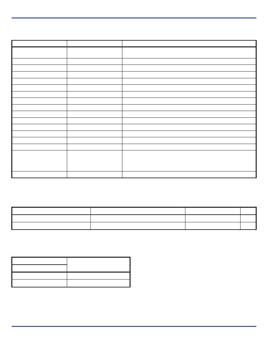
Table 1. Pin Descriptions
NOTE: Pulldown refers to an internal input resistor. See Table 2, Pin Characteristics, for typical values.
Table 2. Pin Characteristics
Function Table
Table 3. Bypass Function Table
Number
Name
Type
Description
1,
2
XTAL_IN
XTAL_OUT
Input
Crystal oscillator interface. XTAL_IN is the input, XTAL_OUT is the output.
3, 32
VCC
Power
Core supply pins.
4, 5
nQC1, QC1
Output
Differential output pair. LVPECL interface levels.
6, 7
nQC0, QC0
Output
Differential output pair. LVPECL interface levels.
8, 16, 25
VCCO
Power
Output supply pins.
9, 10
nQB1, QB1
Output
Differential output pair. LVPECL interface levels.
11, 12
nQB0, QB0
Output
Differential output pair. LVPECL interface levels.
13, 30
VEE
Power
Negative supply pins.
14, 15
nQA5, QA5
Output
Differential output pair. LVPECL interface levels.
17, 18
nQA4, QA4
Output
Differential output pair. LVPECL interface levels.
19, 20
nQA3, QA3
Output
Differential output pair. LVPECL interface levels.
21, 22
nQA2, QA2
Output
Differential output pair. LVPECL interface levels.
23, 24
nQA1, QA1
Output
Differential output pair. LVPECL interface levels.
26, 27
nQA0, QA0
Output
Differential output pair. LVPECL interface levels.
28
VCCA
Power
Analog supply pin.
29
BYPASS
Input
Pulldown
A HIGH on BYPASS signal allows TEST_CLK to propagate to output
dividers and bypass the PLL. a LOW on BYPASS signal allows VCO
frequency to propagate to the output dividers. See Table 3.
LVCMOS/LVTTL interface levels.
31
TEST_CLK
Input
Pulldown
Single-ended input test clock. LVCMOS interface levels.
Symbol
Parameter
Test Conditions
Minimum
Typical
Maximum
Units
CIN
Input Capacitance
4
pF
RPULLDOWN
Input Pulldown Resistor
51
k
Input
Device Configuration
BYPASS
0PLL Mode
1
Bypass the PLL
发布紧急采购,3分钟左右您将得到回复。
相关PDF资料
ICS843156AKLF
IC CLK GENERATOR 32VFQFP
ICS843202AYILF
IC SYNTHESIZER 680MHZ 32-LQFP
ICS843204AGILF
IC SYNTHESIZER LVPECL 48-TSSOP
ICS84320AY-01LN
IC SYNTHESIZER GP LVPECL 32-LQFP
ICS84320AYI-01LF
IC FREQ SYNTHESIZER 32TQFP
ICS843251AG-04LF
IC CLK GENERATOR LVPECL 8-TSSOP
ICS843251AGI-14LF
IC CLK GEN ETHERNET 25MHZ 8TSSOP
ICS843251BGI-12LF
IC CLK GENERATOR LVPECL 8-TSSOP
相关代理商/技术参数
ICS843156AKILFT
功能描述:IC CLK GENERATOR 32VFQFP RoHS:是 类别:集成电路 (IC) >> 时钟/计时 - 时钟发生器,PLL,频率合成器 系列:HiPerClockS™ 标准包装:1,000 系列:- 类型:时钟/频率合成器,扇出分配 PLL:- 输入:- 输出:- 电路数:- 比率 - 输入:输出:- 差分 - 输入:输出:- 频率 - 最大:- 除法器/乘法器:- 电源电压:- 工作温度:- 安装类型:表面贴装 封装/外壳:56-VFQFN 裸露焊盘 供应商设备封装:56-VFQFP-EP(8x8) 包装:带卷 (TR) 其它名称:844S012AKI-01LFT
ICS843156AKLF
功能描述:IC CLK GENERATOR 32VFQFP RoHS:是 类别:集成电路 (IC) >> 时钟/计时 - 时钟发生器,PLL,频率合成器 系列:HiPerClockS™ 标准包装:1,000 系列:- 类型:时钟/频率合成器,扇出分配 PLL:- 输入:- 输出:- 电路数:- 比率 - 输入:输出:- 差分 - 输入:输出:- 频率 - 最大:- 除法器/乘法器:- 电源电压:- 工作温度:- 安装类型:表面贴装 封装/外壳:56-VFQFN 裸露焊盘 供应商设备封装:56-VFQFP-EP(8x8) 包装:带卷 (TR) 其它名称:844S012AKI-01LFT
ICS843156AKLFT
功能描述:IC CLK GENERATOR 32VFQFP RoHS:是 类别:集成电路 (IC) >> 时钟/计时 - 时钟发生器,PLL,频率合成器 系列:HiPerClockS™ 标准包装:1,000 系列:- 类型:时钟/频率合成器,扇出分配 PLL:- 输入:- 输出:- 电路数:- 比率 - 输入:输出:- 差分 - 输入:输出:- 频率 - 最大:- 除法器/乘法器:- 电源电压:- 工作温度:- 安装类型:表面贴装 封装/外壳:56-VFQFN 裸露焊盘 供应商设备封装:56-VFQFP-EP(8x8) 包装:带卷 (TR) 其它名称:844S012AKI-01LFT
ICS8431AM-21
制造商:ICS 制造商全称:ICS 功能描述:350MHZ, LOW JITTER, CRYSTAL OSCILLATOR-TO-3.3V LVPECL FREQUENCY SYNTHESIZER
ICS8431AM-21LF
功能描述:IC SYNTHESIZER GP LVPECL 28-SOIC RoHS:是 类别:集成电路 (IC) >> 时钟/计时 - 时钟发生器,PLL,频率合成器 系列:HiPerClockS™ 标准包装:1,000 系列:Precision Edge® 类型:时钟/频率合成器 PLL:无 输入:CML,PECL 输出:CML 电路数:1 比率 - 输入:输出:2:1 差分 - 输入:输出:是/是 频率 - 最大:10.7GHz 除法器/乘法器:无/无 电源电压:2.375 V ~ 3.6 V 工作温度:-40°C ~ 85°C 安装类型:表面贴装 封装/外壳:16-VFQFN 裸露焊盘,16-MLF? 供应商设备封装:16-MLF?(3x3) 包装:带卷 (TR) 其它名称:SY58052UMGTRSY58052UMGTR-ND
ICS8431AM-21LFT
功能描述:IC SYNTHESIZER 350MHZ 28-SOIC RoHS:是 类别:集成电路 (IC) >> 时钟/计时 - 时钟发生器,PLL,频率合成器 系列:HiPerClockS™ 标准包装:1,000 系列:- 类型:时钟/频率合成器,扇出分配 PLL:- 输入:- 输出:- 电路数:- 比率 - 输入:输出:- 差分 - 输入:输出:- 频率 - 最大:- 除法器/乘法器:- 电源电压:- 工作温度:- 安装类型:表面贴装 封装/外壳:56-VFQFN 裸露焊盘 供应商设备封装:56-VFQFP-EP(8x8) 包装:带卷 (TR) 其它名称:844S012AKI-01LFT
ICS8431AM-21T
制造商:ICS 制造商全称:ICS 功能描述:350MHZ, LOW JITTER, CRYSTAL OSCILLATOR-TO-3.3V LVPECL FREQUENCY SYNTHESIZER
ICS8431AMI-21
制造商:ICS 制造商全称:ICS 功能描述:350MHZ, LOW JITTER, CRYSTAL OSCILLATOR-TO-3.3V LVPECL FREQUENCY SYNTHESIZER